ASE and WUS Invest NT$35 Billion in Taiwan AI Chip Packaging Plant
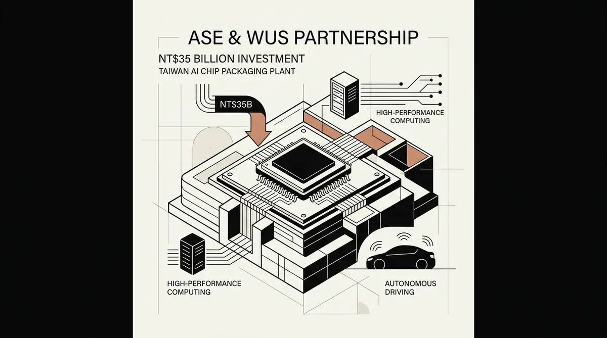
Advanced Semiconductor Engineering (ASE) and WUS Printed Circuit have entered a strategic partnership to build a new manufacturing facility in Kaohsiung, Taiwan, dedicated to AI chip packaging. The project is a total investment of approximately NT$35 billion ($1.1 billion USD) and will be located within the Nanzih Technology Industrial Park. This facility is designed to address the growing global demand for high-performance computing and artificial intelligence hardware by focusing on specialized packaging technologies.
The collaboration aims to finalize construction by September 2029. Once operational, the site will span more than 113,000 square meters. ASE stated that the plant will specialize in Fan-Out Chip on Substrate (FOCoS) and Flip Chip Ball Grid Array (FC BGA) processes. These technologies are essential for the production of hardware used in autonomous driving, cloud computing, and large-scale AI applications. The facility is expected to create over 2,000 jobs and generate an annual output value of roughly NT$16 billion per hectare.
Strategic Importance of AI Chip Packaging
The expansion in Kaohsiung is a direct response to the widening supply-demand gap in the semiconductor industry. As large language models and generative AI tools require increasingly complex hardware, the role of advanced packaging has become a critical bottleneck. Technologies like FOCoS are now industry standards for the high-density interconnects required by modern AI processors. By scaling these capabilities, ASE and WUS are positioning themselves to support the next generation of data center infrastructure.
This move also reinforces Taiwan's central role in the global AI supply chain. The Nanzih Technology Industrial Park is becoming a hub for high-end semiconductor manufacturing, and this NT$35 billion investment highlights the regional commitment to maintaining technological leadership. The partnership combines ASE's expertise in assembly and testing with WUS's capabilities in printed circuit board manufacturing to create a more integrated production flow for AI components.
Beyond immediate production goals, the facility supports long-term trends in autonomous systems and high-performance computing. The integration of FOCoS and FC BGA packaging allows for better thermal management and higher signal speeds, which are necessary for the intensive workloads of 2026 and beyond. As the industry moves toward more modular chip designs, the ability to package multiple dies on a single substrate will remain a key competitive advantage for semiconductor firms.
While we strive for accuracy, bytevyte can make mistakes. Users are advised to verify all information independently. We accept no liability for errors or omissions.
AI-generated image.
Related Articles
- Intel and Musk Unite for $25 Billion Terafab AI Chip Manufacturing Venture
- Intel Surpasses $300 Billion Valuation and Confirms Intel Terafab Partnership
- SUSE and NVIDIA Partner to Deliver Sovereign AI Infrastructure for High-Security Enterprises
✔Human Verified