
Samsung HBM4E: 12-Layer Memory Samples Begin Shipping to Global Customers
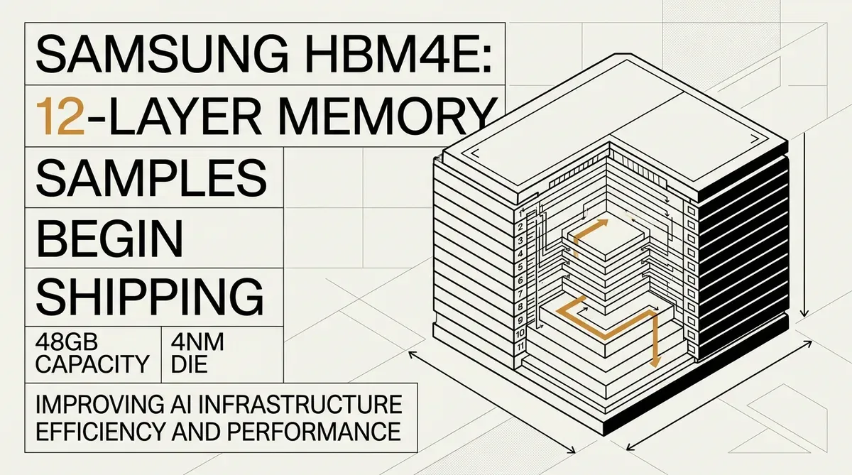
Samsung Electronics has initiated the shipment of the industry's first 12-layer Samsung HBM4E samples to its global customer base. This development, announced on May 29, 2026, is a significant milestone in the high-bandwidth memory market as the demand for advanced AI infrastructure continues to accelerate. The new memory stacks are designed to meet the rigorous performance requirements of next-generation AI accelerators and data centers.
The Samsung HBM4E architecture provides a substantial leap in capacity and efficiency. Each 12-layer stack offers a 48GB capacity, representing a major density improvement for memory-intensive AI workloads. By utilizing a 4nm logic base die, Samsung has achieved a 16% reduction in power consumption compared to previous HBM4 generations. This efficiency gain is critical for enterprise operators managing the escalating energy costs of large-scale model training and inference.
Technical Specifications and Performance
The performance metrics of the Samsung HBM4E samples indicate a focus on both speed and thermal management. The memory features pin speeds that are stable at 14 Gbps, with the capability to scale up to 16 Gbps. This translates to a total bandwidth of 3.6 TB/s per stack. The integration of the 4nm logic die has also allowed for a 14% reduction in thermal resistance, addressing one of the primary bottlenecks in high-density chip packaging.
This release comes at a time of intense competition in the AI memory sector. While competitors like Micron have seen significant valuation growth, Samsung is leveraging its vertical integration to maintain a lead in layer count and architectural efficiency. The transition to HBM4E signifies a shift toward more customized logic dies, allowing memory to be more tightly integrated with the processing units they support.
Strategic Impact on AI Infrastructure
For CTOs and technology strategists, the arrival of 12-layer Samsung HBM4E samples suggests a near-term path toward more capable AI hardware. The increased capacity per stack allows for larger models to be housed closer to the GPU or NPU, reducing the latency associated with off-chip data movement. As AI models grow in complexity, the 48GB capacity per stack will likely become the new baseline for high-end training clusters.
The shipment of these samples indicates that Samsung is moving toward mass production phases. This timeline is essential for hardware partners who are currently designing the next generation of AI accelerators. By providing 14% lower thermal resistance, Samsung is enabling its partners to push clock speeds higher without exceeding the thermal envelopes of modern data center racks.
While we strive for accuracy, bytevyte can make mistakes. Users are advised to verify all information independently. We accept no liability for errors or omissions.
Sources
Samsung Electronics Begins Shipment of Industry-First HBM4E Samples
AI-generated image.
Related Articles
- Samsung Achieves Record Financial Performance as AI Semiconductor Demand Surges
- AI Memory Shortages Drive Long-Term Supply Deals and Surge in Laptop Costs
- Samsung Strike Threat Drives 20% Surge in Memory Spot Prices
✔Human Verified