Tata Electronics and ASML Partnership to Build India's First 300mm Semiconductor Fab
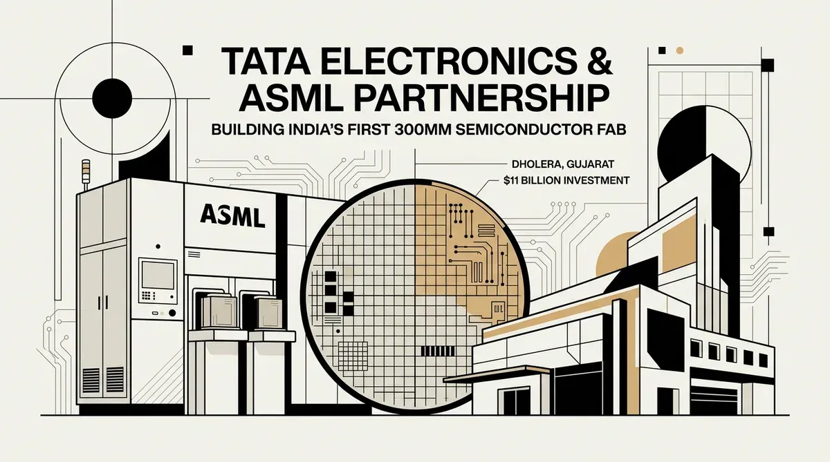
Tata Electronics has entered into a strategic partnership with ASML to support the development of India's first commercial 300mm semiconductor fabrication facility. This Tata Electronics and ASML partnership, announced on May 16, 2026, involves the provision of a full suite of advanced lithography tools and solutions for the upcoming plant in Dholera, Gujarat. The project is a massive $11 billion investment aimed at establishing a domestic supply chain for critical electronic components.
The facility is designed to produce chips at technology nodes ranging from 28nm to 110nm. These specifications target high-growth sectors such as automotive, computing, and telecommunications. By securing ASML as a primary technology partner, Tata Electronics ensures access to the specialized equipment necessary for high-volume 300mm wafer production. The initiative also includes a technology transfer agreement with Taiwan's PSMC, further strengthening the technical foundation of the venture.
Strategic Impact of the Tata Electronics and ASML Partnership
The Tata Electronics and ASML partnership is a significant step in diversifying the global semiconductor manufacturing footprint. Currently, the industry is heavily concentrated in East Asia, which has created vulnerabilities in the global supply chain. India's entry into the 300mm wafer market provides a new alternative for global companies looking to de-risk their hardware sourcing. The Dholera plant is expected to serve as a hub for both domestic consumption and international exports.
Beyond hardware procurement, the agreement focuses on long-term ecosystem development. Tata Electronics and ASML intend to collaborate on research and development infrastructure and talent development programs. This approach addresses one of the primary hurdles in the semiconductor industry: the shortage of skilled engineers capable of operating advanced lithography systems. By building a local talent pool, the partnership aims to sustain the facility's operations and future expansions.
The integration of ASML lithography tools is essential for achieving the precision required at the 28nm node. This specific node is often considered the "sweet spot" for many applications, offering a balance between performance and manufacturing cost. For Tata Electronics, having a direct line to the world's leading lithography provider reduces the risks associated with equipment lead times and technical support, which are common bottlenecks in setting up new greenfield fabs.
Operational Timeline and Technology Focus
The choice of 28nm to 110nm nodes is a calculated move to address the most persistent areas of chip demand. While leading-edge nodes below 7nm capture headlines, the automotive and industrial sectors rely heavily on the 28nm to 90nm range for reliability and cost-efficiency. The Tata Electronics and ASML partnership positions the Dholera fab to capture this essential market segment, providing the "workhorse" chips that power modern vehicles and infrastructure.
Construction and equipment installation are part of a multi-year roadmap intended to bring the facility to operational status. The $11 billion capital expenditure covers the cleanroom construction, the acquisition of ASML lithography stacks, and the integration of PSMC manufacturing processes. This project is a cornerstone of the India Semiconductor Mission, which seeks to transform the country into a global electronics manufacturing destination by the end of the decade.
The Dholera Special Investment Region provides the necessary land and utility infrastructure to support a project of this scale. Reliable power and water supplies are critical for semiconductor fabrication, and the local government has committed to providing these resources to ensure the fab's success. As the first of its kind in India, the facility will likely attract a cluster of ancillary suppliers and service providers, creating a broader semiconductor ecosystem in the region. The first batch of functional wafers is expected to roll off the production line following the completion of the equipment calibration phase.
While we strive for accuracy, bytevyte can make mistakes. Users are advised to verify all information independently. We accept no liability for errors or omissions.
Sources
Tata Electronics and ASML announce strategic partnership
AI-generated image.
Related Articles
- Applied Materials and TSMC Partner at EPIC Center to Advance AI Chip Scaling
- Intel Surpasses $300 Billion Valuation and Confirms Intel Terafab Partnership
- Intel and Musk Unite for $25 Billion Terafab AI Chip Manufacturing Venture
✔Human Verified